13:09
Convert Decimal to any other Base(Binary, Octal, Hexadecimal)| Conversion from One radix to another
Sudhakar Atchala
15:35
Convert Binary to any other Base(Decimal, Octal, Hexadecimal)| Conversion from One radix to another
12:08
Convert Octal to any other Base(Binary,Decimal,Hexadecimal) || Conversion from One radix to another
11:30
Convert Hexadecimal to any other Base(Binary, Octal, Decimal)|Conversion from One radix to another
9:45
Decimal to Binary Conversion || Digital logic design || DLD | Conversion from One radix to another
5:46
Binary to Decimal Conversion || Digital logic design || DLD | Conversion from One radix to another
6:48
Binary to Octal Conversion | Octal to Binary Conversion | DLD | Conversion from One radix to another
6:57
Binary to Hexadecimal Conversion || Hexadecimal to Binary Conversion || Digital logic Design || DLD
6:22
Decimal to Octal Conversion || Digital logic design || DLD || Conversion from One radix to another
5:02
Octal to Decimal Conversion || Digital logic design || DLD | Conversion from One radix to another
11:01
Decimal to Hexadecimal Conversion || Hexadecimal to Decimal Conversion || Digital logic design | DLD
7:13
Octal to Hexadecimal Conversion || Hexadecimal to Octal Conversion || Digital logic design | DLD
15:55
Logic Gates - AND,OR,NOT,NAND,NOR, XOR,XNOR | Truth Table | Digital logic design|Digital Electronics
19:17
Implementation ( Realization ) of all logic gates using NAND gate and NOR gates | DLD | STLD | DE
18:02
Signed and Unsigned binary number representation | Sign magnitude | One's complement | Two's |DLD|CO
3:18
Binary Addition || Binary Arithmetic || Digital logic design | Digital Electronics | DLD | STLD | DE
9:33
Binary Subtraction | 1's | 2's | Complement | Digital logic design | Digital Electronics | STLD | CO
12:34
Binary Subtraction || with borrow ||Digital logic design || Digital Electronics || STLD || CO || DLD
11:28
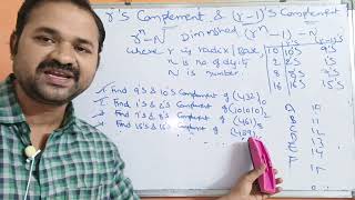
r's and (r-1)'s complement | 1's | 2's | 9's | 10's | 7's | 8's | 15's | 16's | DLD | CO | STLD |DE
15:59
BCD code | BCD Addition | BCD Arithmetic | Digital logic design | Digital Electronics |DLD| STLD |CO
8:22
Gray code || Convert Binary to Gray code and vice-versa || Digital logic design | DLD | STLD | CO
9:07
Excess 3 Code | BCD to Excess 3 code & Vice-versa | Digital logic design | Digital Electronics| STLD
10:27
Excess 3 Addition || Digital Logic Design || Digital Electronics
8:53
Self Complementing Code | Excess 3 | 2421 | Digital logic design | Digital Electronics | STLD|CO|DLD
5:54
Reflective Code || Gray code || Digital logic design || Digital Electronics || DLD || STLD || CO
14:27
Classification of Binary Codes || Digital logic design || DLD || STLD || Digital Electronics || DE
10:46
Basic Laws of Boolean Algebra || Basic Rules of Boolean Algebra || Fundamentals of Boolean Algebra
3:00
Dual of Boolean Expression || Digital Logic Design || Digital Electronics || DLD || DE
15:40
Simplification of Boolean Expressions using Boolean Algebra rules Part 1 || DLD || STLD || CO || CA
18:15
Simplification of Boolean Expressions using Boolean Algebra rules Part 2 || DLD || STLD || CO || CA
33:55
Simplification of Boolean Expressions using Boolean Algebra rules || DLD || STLD || CO || CA
8:32
Minterms and Maxterms in Boolean Algebra || SOP || POS | Digital Logic Design | Digital Electronics
9:57
SOP || POS || Canonical sop || Canonical pos || Sum of products || Product of sum || DLD || DE
5:41
Convert SOP to Canonical SOP or Standard SOP | Express the Boolean Function as a Sum of Minterms
6:37
Convert SSOP to SPOS || Convert SPOS to SSOP || Standard sum of product || Standard product of sum
5:42
Ex 1|Convert POS to Canonical POS|Standard POS|Express the Boolean Function as a Product of Maxterms
Ex 2|Convert POS to Canonical POS|Standard POS|Express the Boolean Function as a Product of Maxterms
8:04
Ex 3|Convert POS to Canonical POS|Standard POS|Express the Boolean Function as a Product of Maxterms
6:32
Ex 4|Convert POS to Canonical POS|Standard POS|Express the Boolean Function as a Product of Maxterms
5:38
Karnaugh Map || K - Map || Digital Logic Design || Digital Electronics
Two Variable Karnaugh Map || 2-Variable K-Map || Simplification of Boolean Expressions || DLD | DE
17:39
Three Variable Karnaugh Map | 3 -Variable K-Map | Simplification of Boolean Expressions | DLD | DE
15:25
Four Variable Karnaugh Map Part 1 | 4 - Variable K-Map | Simplification of Boolean Expressions
11:03
Four Variable Karnaugh Map Part 2 | 4 - Variable K-Map | Simplification of Boolean Expressions
9:47
Four Variable Karnaugh Map Part 3 | 4 - Variable K-Map | Simplification of Boolean Expressions
7:22
Four Variable Karnaugh Map Part 4 | 5 Examples | 4 - Variable K-Map | Simplification of Boolean Ex
8:51
2 Variable K-Map Simplification for POS form || Karnaugh Map Minimization Using Maxterms
7:03
3 Variable K-Map Simplification for POS form || Karnaugh Map Minimization Using Maxterms
7:05
4 Variable K-Map Simplification for POS form || Karnaugh Map Minimization Using Maxterms
9:58
Karnaugh Map with Don't Cares || Don't Care Condition in K - Map Part 1
7:11
Karnaugh Map with Don't Cares || Don't Care Condition in K - Map Part 2
8:59
Don't Care Condition in POS Karnaugh Map || How to solve POS with don't care Conditions
8:06
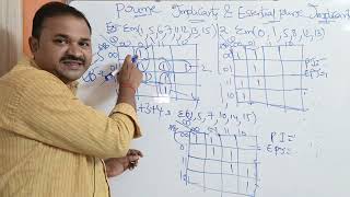
Implicants || Prime Implicants || Essential Prime Implicants || Karnaugh Map || K-Map || DLD || DE
6:39
Prime Implicants and Essential Prime Implicants in Karnaugh Map || K-Map || DLD || DE
7:28
5 Variable K-Map with an example || Five Variable Karnaugh Map || DLD || DE
10:02
5 Variable K-Map with 2 Examples || Five Variable Karnaugh Map || DLD || DE
4:23
Half Adder || Combinational Circuit || Digital Logic Design || Digital Electronics || DLD || DE
6:07
Realization (Implementation) of Half Adder using NAND gate || Digital Logic Design
6:53
Realization (Implementation) of Half Adder using NOR gate || Digital Logic Design
Full Adder || Combinational Circuit || Digital Logic Design || Digital Electronics || DLD || DE
7:59
Realization (Implementation) of Full Adder using NAND gate || Digital Logic Design
10:12
Realization (Implementation) of Full Adder using NOR gate || Digital Logic Design
5:35
Design of Full Adder using Half Adders || Digital Logic Design || DLD
8:17
Parallel Adder || Ripple Carry Adder || Digital Logic Design || Digital Electronics || DLD || DE
4 Bit Binary Adder || Digital Logic Design || Digital Electronics
8:39
4 Bit Binary Subtractor || Digital Logic Design || Digital Electronics
4:01
Half Subtractor || Combinational Circuit || Digital Logic Design || Digital Electronics || DLD || DE
7:00
Realization (Implementation) of Half Subtractor using NAND gate || Digital Logic Design
5:04
Realization (Implementation) of Half Subtractor using NOR gate || Digital Logic Design
10:58
Full Subtractor || Combinational Circuit || Digital Logic Design || Digital Electronics || DLD || DE
12:35
Realization (Implementation) of Full Subtractor using NAND gate || Digital Logic Design
12:21
Realization (Implementation) of Full Subtractor using NOR gate || Digital Logic Design
5:56
1 Bit Comparator || Magnitude Comparator || Digital Logic Design || DLD || Digital Electronics | DE
15:04
2-Bit Comparator || 2 Bit Magnitude Comparator || Digital Logic Design || Digital Electronics
10:56
4-Bit Comparator || 4 Bit Magnitude Comparator || Digital Logic Design || Digital Electronics
Introduction to Multiplexers || 2*1 Multiplexer || 4*1 Multiplexer || DLD || Digital Electronics
8×1 Multiplexer || Digital Logic Design || Digital Electronics || DLD || DE || STLD
7:08
Implementation of 4 × 1 Multiplexer using 2 × 1 Multiplexer || Digital Logic Design || DE || DLD
8:08
Implementation of 8 × 1 Multiplexer using 4 × 1 and 2 × 1 Multiplexer || Digital Logic Design
Introduction to DeMultiplexers || 1×2 DeMultiplexer | 1×4 DeMultiplexer | DLD | Digital Electronics
6:34
Introduction to Decoders || 2 × 4 Decoder || Digital Logic Design || Digital Electronics | DLD | DE
6:31
3 × 8 Decoder || Digital Logic Design || Digital Electronics
4:34
Construction of 3 * 8 Decoder using Two 2 * 4 Decoders | Digital Logic Design |Digital Electronics
9:23
4 * 16 Decoder || Digital Logic Design || Digital Electronics
Construction of 4 * 16 Decoder using Two 3 * 8 Decoders | Digital Logic Design |Digital Electronics
6:21
Construction of 4 * 16 Decoder using 2 * 4 Decoders | Digital Logic Design |Digital Electronics
6:04
Implementation of Full Adder using Decoders || Digital Logic Design || Digital Electronics
Introduction to Encoders || 4 * 2 Encoder || Digital Logic Design || Digital Electronics
8:00
8 * 3 Encoder || Octal to Binary Encoder || Block Diagram || Truth Table || Logic Circuit | DLD | DE
5:28
10 * 4 Encoder || Decimal to BCD Encoder || Block Diagram || Truth Table || Logic Circuit | DLD | DE
4:10
Hexadecimal to Binary Encoder | 16 * 4 Encoder | Block Diagram | Truth Table | Logic Circuit | DLD
13:47
4 Bit Binary to Gray Code Converter || DLD || DE
12:36
4 Bit Gray Code to Binary Code Converter || DLD || Digital Electronics || Digital Logic Design
15:33
4 Bit BCD to Excess 3 Code Converter || Digital Logic Design || Digital Electronics || DLD || DE
17:40
4 Bit Excess 3 to BCD Code Converter || Digital Logic Design || Digital Electronics || DLD || DE
15:00
4 Bit BCD to Gray Code Converter || Digital Logic Design || Digital Electronics || DLD || DE
14:24
4 Bit Gray Code to BCD Converter || Digital Logic Design || Digital Electronics || DLD || DE
11:08
4 Bit Binary to BCD Code Converter || Digital Logic Design || Digital Electronics || DLD || DE
9:55
4 Bit Binary Adder Subtractor || Digital Logic Design || Design Electronics
6:51
Excess 3 Adder || Excess 3 Addition || Digital Logic Design || Digital Electronics
18:01
Carry Look Ahead Adder || CLA adder || Digital Logic Design || Digital Electronics
33:04
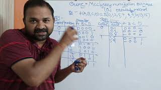
Quine McCluskey Minimization Technique || Example 1 | Tabulation Method | DLD | Digital Electronics
16:47
Quine McCluskey Minimization Technique || Example 2 | Tabulation Method | DLD | Digital Electronics
21:08
Quine McCluskey Minimization Technique || Example 3 | Tabulation Method | DLD | Digital Electronics
10:00
SR latch using NAND gate
8:50
SR latch using NOR gate
10:44
SR Flip Flop using NAND gate
SR Flip Flop using NOR gate
9:37
SR Flip Flop Characteristic Table, Excitation Table & Characteristic Equation
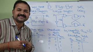
5:44
D Flip Flop || Circuit Diagram || Truth Table || Characteristic || Excitation || Table || Equation
5:48
T Flip Flop || Circuit Diagram || Truth Table || Characteristic || Excitation || Table || Equation
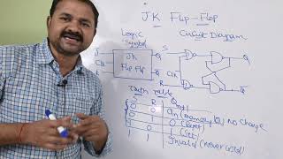
6:49
Introduction to JK Flip Flop || Circuit Diagram || Truth Table || Digital Electronics || DLD
8:28
JK Flip Flop Characteristic Table, Excitation Table & Characteristic Equation | Digital Electronics
Types of Triggering | Edge Triggering | Level Triggering | Digital Electronics |Sequential circuits
3:27
Race Around Condition in JK Flip Flop || Digital Electronics || DLD || Sequential Circuits
4:21
Registers in Digital Electronics || Digital Logic Design || DLD || DE
6:36
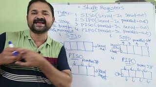
Shift Registers || Types of Shift Registers || SISO || SIPO || PISO || PIPO || Digital Electronics
12:10
SISO Shift Register || Serial In Serial Out Shift Register
SIPO Shift Register || Serial In Parallel Out Shift Register
4:55
PIPO Shift Register || Parallel In Parallel Out Shift Register
15:39
PISO Shift Register || Parallel In Serial Out Shift Register
16:00
Bidirectional Shift Register || Digital Electronics || Digital Logic Design
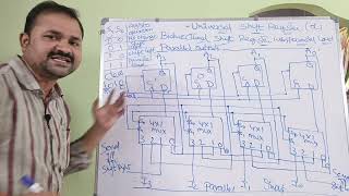
19:09
Universal Shift Register || Bidirectional Shift Register with Parallel Load || Digital Logic Design
5:13
Introduction to Counters in Digital Electronics || Digital Logic Design
7:19
Synchronous vs Asynchronous Counters || Differences || What is ||Digital Logic Design || Electronics
18:24
3 Bit Asynchronous (Ripple) Up Counter || Mod 8 ||Digital Electronics || Digital Logic Design
12:43
2 Bit Asynchronous (Ripple) Up Counter || Mod 4 ||Digital Electronics || Digital Logic Design || DLD
4 Bit Asynchronous (Ripple) Up Counter || Mod 16 || Digital Electronics || Digital Logic Design
6:08
Ring Counter in Digital Electronics || Digital Logic Design
SR Flip Flop to JK Flip Flop Conversion || Digital Logic Design || DLD || Digital Electronics || DE
9:08
JK to SR Flip Flop Conversion || Digital Logic Design || Digital Electronics || DLD || DE
6:16
SR Flip Flop to D Flip Flop Conversion || Digital Logic Design || DLD || Digital Electronics || DE
8:12
D Flip Flop to SR Flip Flop Conversion || || Digital Logic Design || DLD | Digital Electronics | DE
7:17
SR Flip Flop to T Flip Flop Conversion || SR to T Flip Flop Conversion || DLD || DE || Digital Logic
7:27
T Flip Flop to SR Flip Flop Conversion || Converting T to SR Flip Flop || DLD || DE || Digital Logic
4:36
T Flip Flop to D Flip Flop Conversion || T to D Flip Flop Conversion || DLD || DE || Digital Logic
4:44
D Flip Flop to T Flip Flop Conversion || D to T Flip Flop Conversion || DLD || DE || Digital Logic
5:24
JK Flip Flop to D Flip Flop Conversion || JK to D Flip Flop Conversion || DLD || DE || Digital Logic
D Flip Flop to JK Flip Flop Conversion || D to JK Flip Flop Conversion | DLD | flip Flop Conversion
JK Flip Flop to T Flip Flop Conversion || JK to T Flip Flop Conversion || Flip Flop Conversions
6:38
T to JK Flip Flop Conversion || T Flip Flop to JK Flip Flop Conversion || DLD | Digital logic design
8:49
Programmable Logic Array (PLA) in Digital Electronics || DLD | Implement Boolean functions using PLA
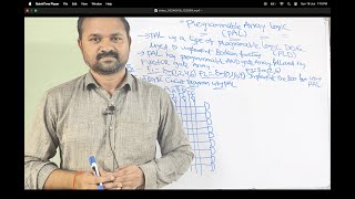
9:02
Programmable Array Logic(PAL) in Digital Electronics || DLD | Implement Boolean functions using PAL
Implementation of Boolean Function using Multiplexers || 8:1 || 4:1 || implementing boolean function
10:08
Implementation of Boolean Function using Multiplexers || 8:1 || 4:1 || Example 2 || Implementing
PROM (Programmable Read Only Memory) || Implementing Boolean Functions using PROM || PROM Example
5:21
PROM (Programmable Read Only Memory) || Implementing Full Adder using PROM || PROM Example2
15:17
Programmable Logic Devices | PLDs | PROM | PAL | PLA | Programmable Read Only Memory | Array Logic
5:20
1 to 8 Demultiplexer | 1 * 8 Demultiplexer | Working | Block Diagram |Truth Table|Boolean expression